BRICC Lab Members Participate in UPWARDS Summer Internship Program at Nagoya University
In August of 2024, two members of the BRICC Lab, Danny Rosen and Kris DeGray, attended the UPWARDS Summer Internship Program hosted by Nagoya University’s Semiconductor Research Lab. Danny and Kris both joined the BRICCs lab in the Spring of 2025 and jumped at the opportunity to participate in this unique experience. Four students from University of Washington, Boise State University, and Rochester Institute of Technology accompanied Virginia Tech’s representatives.
UPWARDS is an international program created in May of 2023 by Micron and TEL. The $30 Million initiative consists of 11 universities. The object of this program is to bring together leading academic researchers in Semiconductor Research to promote advancement in chip manufacturing and foster collaboration between universities. Yang "Cindy" Yi has spearheaded Virginia Tech’s active participation in the UPWARDS venture by hosting a 2 week Summer Camp for Women in Semiconductor Research.
Iconic University

Nagoya’s Historic Campus is Centered around a building funded by the Toyota corporation
Nagoya University is a global leader in Semiconductor research. Co-located in the Aichi prefecture with Japanese manufacturing giants like Toyota and Makita, NU has unequaled exposure to global engineering leadership. The institution has taken full advantage of this access. Six professors from the university have received Nobel Prizes in the 21st century. Among these is Prof. Hiroshi Amano, is laid the foundation for modern Blue LED devices. NU continues to produce cutting edge research in the field. This effort is guided by current professors Jun Suda, Osamu Nakatsuka, Kenji Ishikawa, and Katsunori Makihara. These leading researchers served as instructors during the Internship.
Hands On

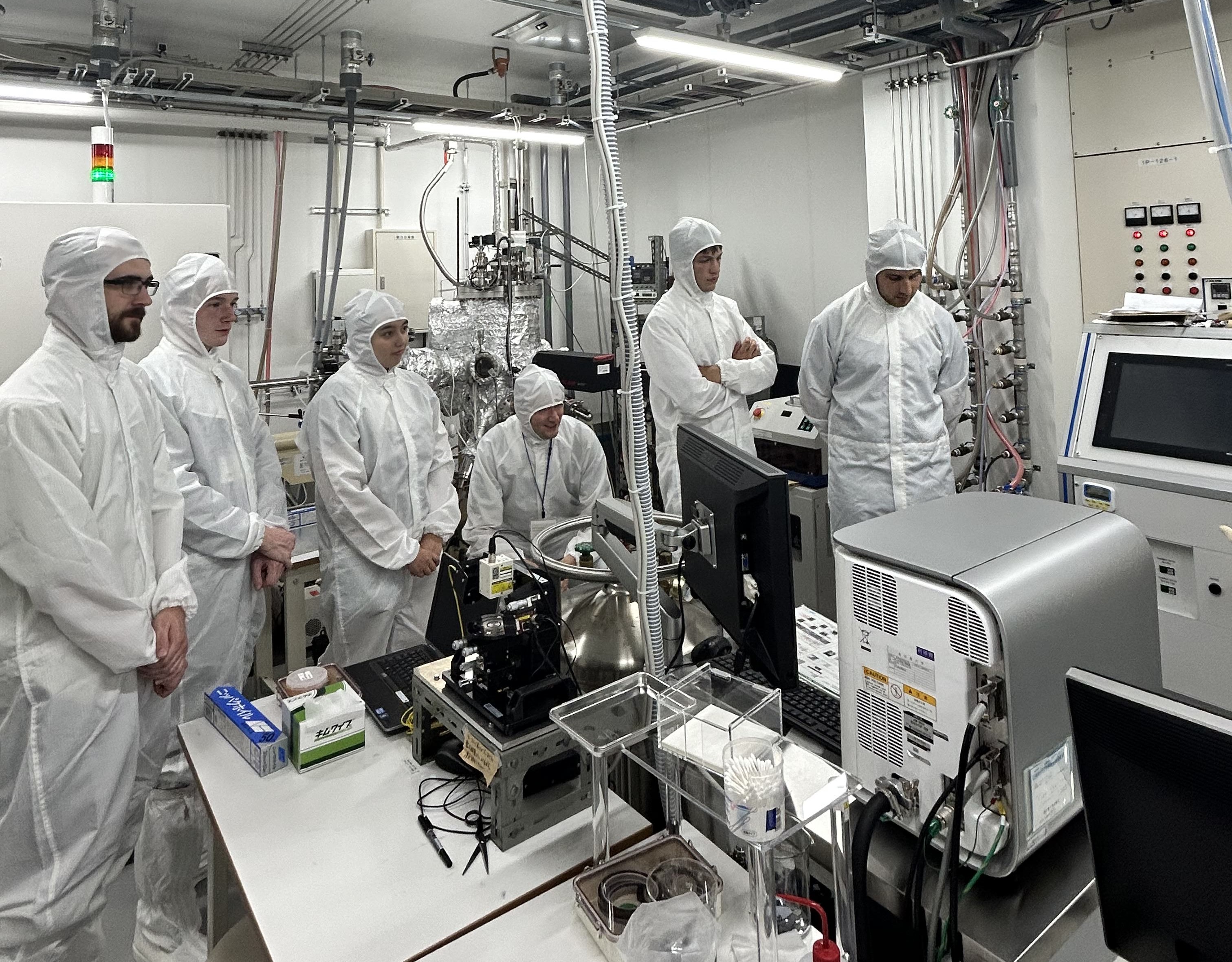
The six interns wear “bunny-suits” to prevent contamination when touring clean rooms
After arriving in Japan, American students were given in-depth tours of the advanced lab equipment on campus.
On the first stop, Danny and Kris toured the Center for Integrated Research of Future Electronics (CIRFE). This facility conducts experimentation on Gallium Nitride (GaN) Semiconductors. This material is optimal for high-voltage systems like Vehicles or Aircraft. Later, students performed quantitative analysis on the hardware produced using these techniques.
One fundamental challenge of chip manufacturing is accurate etching of circuits. At the atomic scale, highly accurate, efficient material removal becomes very difficult. Plasma etching may be the optimal solution to this problem. Prof. Ishikawa’s lab leads advancement on this technology. Students visited this lab to get a glimpse of the future of plasma etching.

The students combined the diodes to create a circuit that used energy from the sun to play music
Danny examines the result of the Chemical Vapor Deposition
The educational experience was capped by a workshop in the National Innovation Complex. With all this new knowledge, the Interns were tasked with the creation of their very own semiconductor devices. Danny and Kris performed chemical deposition, oxidization removal, and quantitative analysis of their own diodes. These were then used to create a solar cell!
Industry Experience

Students are briefed on the technology involved in producing synchrotron radiation.
In addition to academic experiences, visiting students were exposed to industry-centric initiatives for semiconductor advancement.
Danny and Kris visited the Aichi Synchrotron Radiation Center. Housed in this Facility is a particle accelerator used for microanalysis of semiconductor materials. By accelerating particles in a non-linear path, highly measured light radiation can be produced for analyzing materials at a very small scale.
The group then moved to the Denso corporation’s Aichi Location. This facility produces chips for Automobiles. Students, toured their manufacturing process, met with leadership, and learned about the unique engineering challenges necessary for managing an advanced material of this kind.
Warm Welcome
The Virginia Tech students were deeply immersed in Japanese culture during their trip. Nagoya University students accompanied their guests on various historical and cultural outings. Language barriers quickly dissolved as individuals from opposite ends of the earth bonded over shared music, food, and pop culture tastes.
Students try new foods on a Shabuki grill

Interns take a trip to Nagoya’s centuries-old Castle from the Edo Period
The cohort took an excursion to Nagoya Castle, a historic structure dating back to Japan’s Edo Period. Additionally, students dug in to several traditional meals like Shabu Shabu and Izakaya. They were also treated to a demonstration of Karakuri dolls, a traditional Japanese marionet.
On this aspect of the trip, Kris DeGray says, “The Japanese students were awesome. Not only did they help with the material that the program teaches but they are great teachers about the cultural differences between the U.S. and Japan. I still keep in contact with some of them outside of an academic context. The program wouldn't be half of what it is without them."
More to Come!
The MICS Lab at Virginia Tech looks forward to the continued relationship between Blacksburg and Nagoya. This trip is only the beginning of ongoing collaboration between the two universities.
Regarding this new connection, Dr. Cindy Yi says, “I am so grateful for Nagoya University for opening its doors to Virginia Tech students. The MICS lab looks forward to sharing ideas and working together for the advancement of semiconductor research.”


